Ångström Space Technology Centre
Microsystems Technology, Department of Engineering Sciences, Uppsala University
Contact: Ass. Prof. Greger Thornell
www.astc.uu.se
The Ångström Space Technology Centre (ÅSTC) has a staff of ten people running roughly the same number of major projects, most of which develops and studies microdevices for aerospace and other demanding applications. Since its start in 2000, ÅSTC has participated in ten major European collaborations, and several national & bilateral projects, and delivered nine PhDs and more than 150 journal and conference papers. ÅSTC works multi- and interdisciplinary and is very application oriented. With respect, in particular, to the process part, it is the main user of the MSL node of Myfab.
Making up kind of a matrix, research is conducted both on several technological and scientific levels, and in various fields of application. The below examples from ongoing studies are chosen to illustrate this.
Miniature Submersible
The Deeper Access, Deeper Understanding endeavour aims at developing an underwater vehicle the size of two small soda cans, stuck together end to end, to enable its deployment through, e.g., glacial boreholes to lakes housing pristine flora and fauna under kilometres of ice. Besides the study of vehicle issues: control system, navigation, propulsion, hull design etc, much attention has been paid to the onboard instruments. Among these, the world’s smallest side scanning sonar, which enables detailed imaging in pitch black or turbid water, and a laser-based topography measurement system have been developed. Still ongoing subprojects are, e.g., power transfer via an optical fibre tethering the craft to a ground station, and a water sample enrichment device based on acoustic particle trapping.
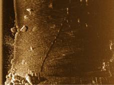
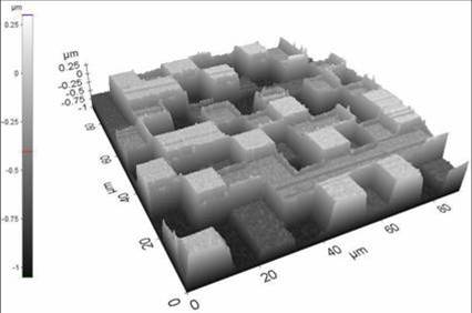
Image from sonar field testing revealing a cable, rocks and a school of fish (left). Part of a diffractive optical element enabling the laser projection of a completely different reference pattern, as viewed with an atomic force microscope (right).Nanoengineering for Materials Property Analysis and Sensing
Magnetometer for Small Satellites
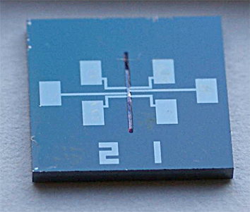
Employing a stack of extremely thin layers of carefully selected materials, patterned with beams of highly energetic ions into patches a few micrometers wide, very sensitive and quickly responsive elements converting magnetic field fluctuations into changes in tunnelling resistance can be manufactured. By a multitude of such sensors arranged and connected appropriately, a magnetometer can detect the strength and direction of some of the faintest whims of magnetic fields in space. The small size of the sensor elements themselves, and, equally important, the supporting electronics, makes this an instrument affordable by mass even on extremely small satellites.
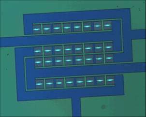
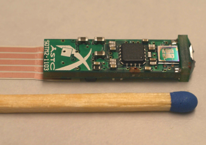
Arrangement of microsized tunneling junctions for magnetic field measurements (left). Final magnetometer including electronics (right).
High Temperature Microfluidics
No matter if it’s for high-performance microrocketry or for fluid sensors in combustion engines or high-temperature reactor chemistry, conventional silicon devices start to yield at temperatures fairly far below their melting point. This softening need not be accompanied by an external force to result in deformation and component failure. Thermal mismatch of, e.g., materials for electric connection, e.g., bonded to, embedded in, or deposited on top of, the silicon is often a reason enough. At ÅSTC, the challenge is approached in two generically different ways. One is based on oxidizing silicon to an extent allowing for robust, all-oxide structures and locating hotspots to certain regions of the devices. The other is to work with fine-grained ceramics structured by silicon masters.
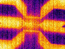
Non-connected flow sensor made by thick oxidation of silicon (left). IR image of ceramic flow sensor with heat spreading from the middle heating element sandwiched by similar temperature gauges (right).